|
|
Comparative Test: HTS 81 Original vs. Plagiarism |
 |
|
Parameter |
IMITATED
MOSFET SWITCH Specified for 8 KV operating voltage and 15 A peak current, manufacturing date unknown, purchased in 2011. Note: All information published here refer to this specific sample and to the date of purchase of this sample. |
ORIGINAL BEHLKE MOSFET SWITCH 8 kV operating voltage and 30 A peak current, old version of the model HTS 81, still without VC4 and manufactured in 2009. Note: The outdated HTS 81 is not recommended for new developments. Please use model HTS 101-03 for new designs. |
|
| 1 | Housing dimension | The data sheet promises the same dimension as the original Behlke switch (89 x 64 x 27), but in reality it is 89 x 64 x 31 mm. | HTS 81, old version: 89 x 64 x 27 mm, new version: 89 x 64 x 22 mm, respectively 89 x 64 x 17 mm with option FC (flat case). |
| 2 | Housing material | Black thermoplast, ABS, flammable, maximum useful temperature 70°C (158F). |
Black duroplast, Diallyl Pthalate, flame
retardant according to UL-94 V0, temperature proof up to 260°C (500F). |
| 3 | Casting Resin | Black mat surface. The quality of the potting can not be verified by view, since possible surface bubbles are removed by milling. | Black, glossy and bubble-free surface thanks to a widely automated vacuum potting process. |
| 4 | Marking | Ink-jet printed paper label with model reference and warning hint. Tracking not possible due to missing serial no. Paper label is flammable and detaches from the surface during warm-up. | Laser marked plastic foil, flame retardant according to UL-94 V0, with model reference, serial no, manufacturing date, ratings, pinning, safety hints, short instructions and over temp. indicator. |
| 5 |
High voltage switch technology |
X-ray images show a circuit, which is one to one identical to an old Behlke patent (DE3630775, claim 3). Note: This circuit has never been used by Behlke in the archetype form. The simple archetype circuit utilized in the present plagiarism was not intended by Behlke for professional applications! | Advanced proprietary Behlke technology. |
| 6 | HV connectors | 2 tiny breakable soldering pins at the front side with the same polarity as the original Behlke switch. |
2 massive soldering pins at the front
side. Left is HV minus, right is HV plus. New models have screw
terminals at bottom. |
| 7 | Earthing / ground connector |
No earthing terminal at all. In case of
an insulation failure, the entire energy from the HV circuit is
dumped directly into the control circuit of the application! High
risk of electrical shocks! |
1 massive soldering pin for earthing in the middle of the front. Serves also as a well defined star-type ground terminal for good EMC behavior in applications with high di/dt and high dv/dt. |
| 8 | Control connector | Open wires for auxilliary supply, coaxial socket for control input. The switch cannot be operated without input shielding! An unshielded input may damage the switch in high voltage operation due to uncontrolled switching of the individual MOSFET's (see also # 14) | MOLEX plug, TYCO plug since 2005. Due to active input filters, the HTS 81 does not need any shielded input wiring under normal operating conditions. In critical situations with high external noise level a shielded input is available as option LS-C. |
| 9 | Auxilliary Supply | +5.00 VDC (±5%), 500 mA at a operating frequency of 30 kHz. | +5.00 VDC (±5%), 500 mA at a operating frequency of 40 kHz. The HTS 81 for 15 A (pk) consumes 500 mA at 80 kHz. |
| 10 | Max. switching frequency | 30 kHz according to the data sheet. The specification is very unrealistic, since the frequency is limited first of all by the max. power dissipation of the switch. According to the present data sheet, the max. power dissipation of the plagiarism is only 33 % of the Behlke original switch, which has 15 Watts since 2002. | The max. switching frequency with the internal DC/DC converter is 40 kHz for the standard models with 30 A and 80 kHz for the models with 15 A. In connection with option HFS (ext. supplies) and sufficient cooling options (e.g. option CF, ILC or DLC) the continuous switching frequency can be increased up to 3 MHz. |
| 11 |
Noise from the internal DC/DC converters |
50 mVpp 25 mVpp at 0 Hz switching
frequency, measured at the 5 V input, in 75mm distance from the
housing. |
25 mVpp at 0 Hz switching frequency, measured at the 5 V input, in 75mm distance from the housing (newer models: <10 mVpp) |
| 12 |
Noise from the
internal driver clock |
No synchronization between trigger and driver clock. The clock is free running during the on-state and generates permanently heavy noise transients. | The first 500 µs of the HV pulse are absolutely noise free due to proprietary synchronization circuit, which sychronizes trigger and clock. A zero noise option is also available. |
| 13 | Peak current and breakdown voltage |
The imitated switch has 9 MOSFET (in
series only), resulting in a nominal breakdown voltage of > 9 kV
and a nominal peak current of 15 A. |
The original HTS 81 has 20 MOSFET (10 in series, 2 in parallel). The peak current is therefore 30 A and the nominal breakdown voltage is > 10 kV. The HTS 81 is also optionally available with only 10 MOSFET for 15 A peak current and 80 kHz rep. rate. |
| 14 | Turn-on rise time | Turn-on rise time with resistive load is 9.3 ns at 5 kV. |
Turn-on rise time with resistive
load is 6.1 ns at 5 kV. |
| 15 |
Input noise immunity and reliability at
undefined control signals |
The imitated switch is extremely noise sensitive. There is no efficient input filter against feed-back effects. Fast switching (without capacitive load) is impossible, if the control input is not shielded perfectly. Undefinded control signals are not conditioned by the control electronics. In case of an undefined control signal, the stacked MOSFETs will not switch synchronuously, which can lead to a catastrophic switch failure, especially if the maximum avalanche energy of a single MOSFET is exceeded. The data sheet of the imitated switch says, "a control pulse width of less than 50 ns can result in unpredictable switch behavior". This means in reality, the switch can be damaged, if pulses or transients shorter than 50 ns are applied to the control input. |
Due to an active input filter, the switch
can be safely operated with unshielded input wires of at least 25 cm
length (10 inch). Shielded cables are normaly dispensable at short
distances between switch and control electronics. A shielded wiring
is only required in case of very difficult noise environments or in
case of pulse transmission over long distance. The switch can then
be optionally equipped with an shielded LEMO input (option LS-C). Behlke switches
have always
an active signal conditioning circuit at the input, which avoids undefined
switching of the individual MOSFETs under all circumstances. In
contrast to the plagiarism, the original Behlke switch can not be
destroyed by feedback
effects, undefined signals or too short control pulses.
|
| 16 | High voltage transients | Since the imitated switch utilizes an outdated and very simple technology from an old Behlke patent, the switch is not transient proof. It may be damaged at HV slew rates of > 100 V / us. | The original Behlke switch withstands high voltage input transients and fluctuations with a slew rate of > 1kV / ns. The HV can be applied to the switch input very rapidly without any risk. |
| 17 | Monitoring features |
The imitated switch has obviously no
special monitoring circuits. The data sheet mentions a
thermotrigger, but the test sample was thermally destroyed after 23
minutes at max. rated current. |
The original HTS 81 has internal monitoring functions to protect the switch against damages from over frequency, over temperature and incorrect auxilliary voltage. |
| 18 |
Power dissispation, continuous current and thermal test |
The data sheet
of the imitated switch promises > 0.5 A continuous current at 25°C
ambient temperature, but there is already a mathematical
contradiction between the Pd(max) and the on-resistance
specification, which completely ignores the positive temperature
coefficient of the MOSFETs Rds(on). In the present case the resulting power dissipation at 25°C ambient temperature and a constant current of 0.5 A will therefore be up to three times higher than the max. power dissipation specified in the data sheet, if the positive temperature coefficient is taken into account. It was therefore not surprising that the surface temperature exceeded 150°C after 20 minutes, when a continuous current of 0.5 A was applied. The high voltage section was completely destroyed after 23 minutes and the cheap ABS housing began to burn. Luckily the flammable paper label fell off during warm-up. The thermo trigger did not respond. Conclusion: High risk of fire at overload conditions due to a nonfunctioning thermotrigger, highly flammable housing materials and false specifications. 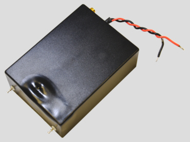 Fig 1: The imitated switch after testing with 0.5 A continuous current for 23 minutes. The switch has been completely destroyed in the high voltage section. The ink-jet printed paper label has been fully detached during warm-up. |
The data sheet
of the standard Behlke switch (without cooling options) allows 0.45
A continuous current if the housing surface temperature is kept
below 25°C (e.g. by forced convection). To prove this very conservative specification, a continuous test current of 0.5 A was applied for 120 minutes without any forced cooling. The heat was removed by natural convection only. As expected, the average temperature of the module reached a critical level after two hours, but the average temperature was still below the thermotriggers threshold. The surface temperature reached 103°C in the center of the heat dissipation zones, but without any electrical or mechanical damage to the module. Thanks to the temperature proof and flame retardant duroplast housing, there is no risk of mechanical damage or fire at overload conditions. Thermal switch damages are avoided by a reliable thermotrigger with short response time. 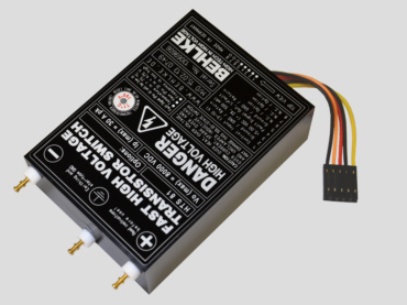 Fig 2: The original Behlke switch after testing with 0.5 A continuous current for 120 min. No electrical or mechanical damages: Clearly visible quality from the inventor of the fast high voltage solid-state switch. |
| 19 | Warranty | 90 days (does not comply with the warranty law of most countries) | 5 years worldwide |